Date: Fri, 14 Dec 2012 14:44:56 +0400
Hi I am trying calculate electronic damages when 20 Mev (or greater )
electron beam hits a sample target (Silicon).
I carefully red the article and tried to implement it myself.
http://info-fluka-discussion.web.cern.ch/info-fluka-discussion/lectures/Damage2Electronics.ppt
Now I have couple of question regarding to that
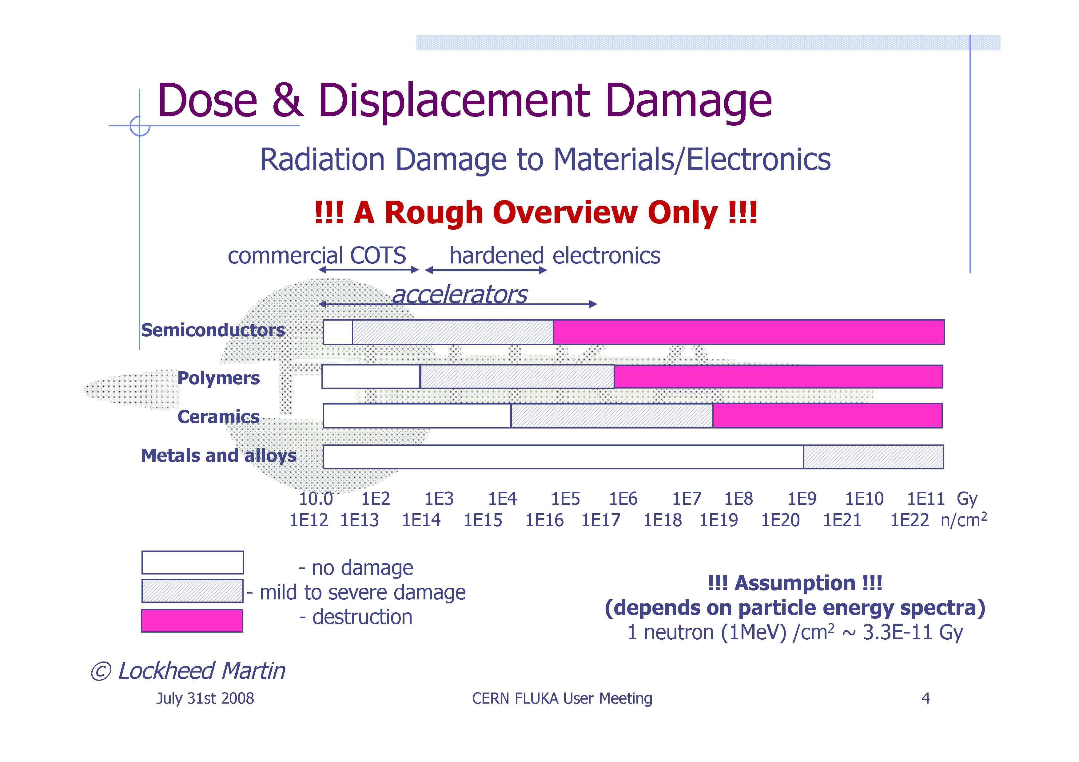
1) Are the damage threshold ranges ( given in Gy, n/cm^2) for various
types of materials per year? ( See Attached Image)
1.1) If so, does it mean that materials will be damaged if they
exposed to a given level of dose Continuously during one year?
"I mean, can one Second exposure ( which is equivalent to
that dose level per year) create damages?
1.1.2) As I understand output units of USERBIN and USERTRACK
cards (/with type SI1MEVNE, ///HADGT20M//) cards in [neutron/cm^2] and
[hadron/cm^2] . Am I right?
As I understood in order to calculate damages I should do following steps
1) Do calculation USERBIN and USERTRACK cards with part. type
Dose/, //SI1MEVNE/and //HADGT20M//
2) Take values from plots of that cards
3)Compare plots values with the chart that I attached ( See
Attached Image)
Generally my question is:
1)How should I use data of USRTRACK(with part type //SI1MEVNE,
HADGT20M//) card in order to figure out, is material (for example
Semiconductor) in a given region damaged or not/?
(the same is about USERBIN card )/
1.1) It is not clear. How should I calculate and define
Stochastic failure happens or not?
1.1.2) Is it done via //scoring/quantity /HADGT20M//and how?
" I mean from where I can get dose (or fluence)
approximate thresholds of Stochastic failures of materials, (like in
Attached Image)? "
I ask experts If you have time can you take a look to my input card and
say what I miss or did wrong?
//
Many Thanks!
//
- application/x-fluka attachment: damage.inp