Date: Sat, 24 Jan 2009 12:00:05 +0100
Dear Paola. Indeed there was an obvious mistake in the geometry that I
did not spot. I must admit that I did not run a proper geometry debug
check my self. Thank you for pointing that out. I therefore moved the
XYP SBUMP plane from 9.005e-4 cm to 9.02e-4 cm in order to avoid the
overlap with the voxels. A geometry debug check in the region
x: -0.001 to 0.01 with steps 1000
y: -0.001 to 0.01 with steps 1000
z: -0.001 to 0.001 with steps 1000
ran successfully without reporting any errors.
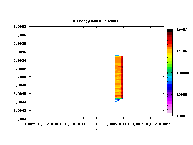
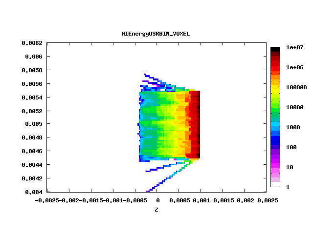
I then repeated the runs for the Mg24 beam and I believe the result
turned out similar to the runs with the erroneous geometry. (see
attached plots). Again, the Mg24 beam seems to have a longer range when
the voxels are present compared to when they are not.
Regarding the cpu time using the EVENTBIN, I have attached a plot
(cputime.pdf) showing the relationship in reported cpu time per particle
(from the standard output file) for 3 different implementations of the
EVENTBIN, and for 4 different runs of 10e3 ,10e4, 10e5, 10e6 primary
particles. As you can see when no EVENTBIN is activated the cpu time per
particle is ~1ms, when a 235x235x5 mesh EVENTBIN is used the cpu time
increase to ~6ms and for 235x235x10 it increases again to ~12 ms. If you
need to run 10e8 primaries this difference in total simulation time
between no EVENTBIN and the 235x235x10 case is in the order of days.
The simulation is done with similar geometry as for the case above. To
check if the geometry error made a difference I removed the voxel
implementation and repeated the runs for the first case of using 10e3
primaries and ended up with very similar results. I did not use the
fastest PC in the world for these simulations (PIII 1.3 MHz), but it was
the relative difference and not the absolute time that was important for
this test. I have attached the input files I have used for the 3 cases.
Best regards,
Ketil
Paola Sala wrote:
> Dear Ketil,
> there is a problem in your geometry with voxels: the voxel parallelepiped
> overlaps with the "sbump" region
> ( it is 9E-4 cm long, and starts at z=1.E-6 ==> it extends to z=9.01e-4,
> crossing the plane at 9.005E-4). I made a geometry debug, getting
> **** Lookdb: Geometry error found ****
> **** The point: 0.0010000001 0.001 0.0009005 ****
> **** is contained in more than 1 region ****
> **** (regions: 8 SBUMP 11 VOXEL002 ) ****
> and so on
>
> please correct the geometry and try again. If the strange behaviour
> persist, let me know.
> Paola
>
>
>
>> Dear All,
>> I need some feedback on a type of simulation I would like to
>> carry out using fluka. The simuation problem I am working on is
>> related to Single Event Upsets (SEU) in SRAM based memory cicuits.
>> The main purpose of the simulation is to see if it is possible to
>> reproduce the SEU cross section results from irradiation tests of an
>> SRAM based memory device. And, if this is possible to do using fluka.
>> The beams of interest are protons of 30 and 150 MeV.
>>
>> The approach taken is a based on a fairly simple methodology which has
>> shown to give reasonably good results by others. If this methodology
>> is still valid with the decreasing feature sizes of modern
>> semiconductor devices, is a separate discussion. For now I therefore
>> assume that the below described RPP methodology is valid for my case.
>>
>> An SEU can be defined as a bitflip in a memory cell caused by charge
>> deposited in the sensitive volume of this memory cell by a single
>> ionizing particle. In order to cause an SEU the charge deposited
>> (Qdep) must be larger than a given critical charge (Qcrit)associated
>> with the memory cell. In a chip of millions of memory cells not every
>> memory cell is identical and thus the Qcrit is not 1 value, but a
>> distribution of values.
>>
>>
>> The methodology is based on describing the sensitive volume of a
>> memory cell as a rectangular parallelpided volume (RPP). Simplified,
>> by simulating the charge deposited within this volume and comparing
>> the result to the distribution of Qcrit, the number of SEUs generated
>> equals the number of charge depositions larger than the Qcrit.
>>
>> To do this in fluka I have tried to build a geometry that in a
>> best possible way represents the real structure of a typical
>> chip. To simplify, I assume that the memory cells are evenly
>> distributed over the full chip in a periodic fashion. Only a small
>> sample of the real size is therefore used. The area is approx. 100 x
>> 100 um and the thickness is approximately 1400 um. In the fluka
>> simulation setup the thickness is along the z-axis/beam axis. A simple
>> schematic of the geometry is shown below.
>>
>> ------> Z
>> 450um 850um 1um 9um 100um
>> ------------------------------------------------
>> | | |*| | |
>> | | |*| Inter | |
>> p--> |Cu Lid |Si substracte |*| connect| Package | 100um
>> | | |*| layers | substrate |
>> | | |*| | |
>> ------------------------------------------------
>>
>> The layer denoted by stars are where the memory cells are located in
>> the chip. That is, this is the area where the scoring of deposited
>> charge should take place. Just after, alternating layers of
>> copper interconnect wires and dielectric follow. At the end is the
>> package substrate which in some cases consists of a flip chip solder
>> bump (Sn/Pb mixture).
>>
>> I do not have the detailed layout of the chip and in particular the
>> interconnect layers. I therefore base my geometry on a simple
>> structural examination of the chip. This has allowed me to retrieve
>> for instance the thickness of each interconnect layer, but not the
>> detailed layout of the copper wiring. Due to the periodic nature of
>> the chip I again assume that the fraction of copper wires is evenly
>> distributed. I therefore assign a fraction(0-100%) of copper to
>> dielectric (SiO2) in each layer. A typical copper wire thickness in my
>> case is approx. 0.5 um thick. To accommodate this granularity I have
>> utilized the Voxel geometry available in Fluka to build the different
>> layers. Each layer contains a number of copper voxels corresponding to
>> the fraction of copper assigned for that layer. The Voxels are
>> randomly distributed in each layer. For now this seems to be the best
>> solution I can come up with when the layout information is not known.
>> To some extent I believe this approach should
>> caputure the granularity of the interconnect layers compared to only
>> using a uniform layer of a material.
>>
>>
>>
>> So far this has been a short introduction to my case study. In the
>> following are more fluka specific issues where feedback will be greatly
>> appreciated.
>>
>> To score the deposited charge by a single particle I believe the
>> EVENTBIN scoring card is appropriate. An advantage of using EVENTBIN
>> is that by making a mesh of small sized bins, different sizes of
>> sensitive volumes can be achieved by combining the result from various
>> bins. This is particulary valuable when the actual size of the
>> sensitive volume is not known. Instead of implementing different sizes
>> of the sensitive volumes as geometry, and then running several
>> simulations for each size, this analysis can rather be done in the
>> post-processing stage. EVENTBIN scoring is also an easy method to
>> utilize several sensitive volumes in order to increase the collection
>> statistics. Because the expected sensitive volume size is close to
>> 0.4 x 0.4 x 1.0 um^3, I would like to use bins of size 0.2 x 0.2 x 0.2
>> um^3. This means that a single sensitive volume is built of several
>> bins. The critical charge/energy in my case is in the order of 10 fC
>> or ~0.2 MeV.
>>
>> The main suspects to cause an SEU for this device technology are the
>> highly ionizing fragments produced in inelastic nuclear reactions. In
>> particular the alpha-particle and residual ion are important.When
>> produced in an inelastic reaction from a 30 MeV proton on Si, the
>> typical fragment energy is approx. 5 MeV and below for alpha, and 1
>> MeV and below in the case of the residual ion (i.e. Mg24). Using SRIM
>> the corresponding range in Si is found to be approx. <25 um and <1-2
>> um respectively. Thus, only fragments produced close to the layer of
>> sensitive volumes will contribute to the SEU rate.
>>
>> 1a) How does fluka treat the residual ion? In the manual it says that
>> when an ion is below the transport threshold it is ranged out to
>> rest. Does this mean that if the range crosses a scoring bin, the
>> energy deposited is calculated as given by slide 18 in
>> http://www.fluka.org/content/course/NEA/lectures/Transport.pdf
>> [(dl/dx)*dE]
>>
>> 1b)
>> Can an ion that is ranged out be scored by using the AUXSCORE card
>> for HEAVYION combined with EVENTBIN? Or is this only possible when the
>> particle is transported?
>>
>>
>> 1c) Can a few MeV ion be transported until it has lost all its energy
>> by reducing the PART-THRES for HEAVYION? From the manual this does not
>> seem to be true. The limits are given as 10MeV/n and 100MeV/n
>> for transport of secondary and primary heavy ions
>> respectively.
>>
>> However, I still seem to be able do some kind of
>> transport of a Mg24 ion. But maybe the transport limit is the
>> reason why I do not understand my resuls. See
>> information/question further below.
>>
>> 1d) With sub-micron scoring bin size, does fluka still give valid
>> results for energy deposition? If possible, what type of
>> physics/transport settings should be used to optimize for this type of
>> simulation?
>>
>>
>>
>> **************************************************************************
>> Using EVENTBIN scoring increases the simulation time. Also, due to the
>> low probability of inelastic reactions a large number of primaries are
>> needed to achieve reasonable statistics. Because the EVENTBIN scoring
>> writes an entry to the log file for every event, in my case, this
>> results in log files of several GB. Also the expected simulation time
>> can reach several days to weeks depending on computer specifications and
>> wanted statistics.
>>
>> 2a) I understand that it is possoble to score only bins with hits.
>> However, even if there are no hits, a line giving the event number and
>> number of hits is still written to the EVENTBIN output. Is there any
>> way that the latter can be avoided? Is there are reason for writing an
>> entry for events that have no hits, or is this in fact redundant
>> information?
>>
>>
>> In order to minimize this problem I have tried to divide the
>> simulation in two steps. First I run a simulation to locate all
>> inelastic reactions and store information about the produced
>> fragments. This is done by the USDRAW routine in mgdraw.f. By
>> optimizing the simulation for this task and not using any other
>> scoring, this reduces the simulation time significantly. However, no
>> biasing is used since this is not recommended in combination with
>> EVENTBIN scoring. The optimization is simlply done by minimizing the
>> transport of all other particles except the primary proton. In the
>> second step, the source.f routine is used to transport only the
>> fragments of interest produced in the inelastic reactions and score
>> them using EVENTBIN. This greatly reduces the size fo the EVENTBIN log
>> file.
>>
>> When doing this exercise, I noticed some results that I could not
>> explain. I therefore need someones feedback on the following
>> simulation results.
>>
>> Starting from the right side of the interconnect layers (in the
>> package substrate) a beam of either 10000 5 MeV alpha-particles or
>> 5e-5 MeV (~1.2MeV/n) Mg24 ions are directed towards the interconnect
>> layers (negative z-direction).
>>
>> -----> Z
>> 450um 850um 1um 9um 100um
>> ------------------------------------------------
>> | | |*| | |
>> | | |*| Inter | |
>> |Cu Lid |Si substracte |*| connect| <-- He4 |
>> | | |*| layers | Mg24 |
>> | | |*| | |
>> ------------------------------------------------
>>
>>
>> Two cases are simulated for each beam, one with the voxel geometry
>> implemented, and one without the voxel geometry but with a layer
>> of only SiO2 instead.
>>
>> For the alpha-particle I got what I judge as an expected results. When
>> the layer contains the voxels of copper more energy is deposited which
>> in turn slightly decreased the range of the alpha-particle beam.
>>
>> What I do not understand is that I did not see the same behaviour when
>> I instead
>> used a Mg24 beam. Infact, I observed the opposite. The beam
>> seemed to reach further when the copper voxels were present compared
>> to when they were not. When only a layer of SiO2 was used the fluence
>> and energy plot shows a that the beam reaches approx. a few
>> microns. Compared to what SRIM predicts this sounds reasonable. However,
>> with
>> the copper voxels in the beam path, the fluence and energy plot
>> reached almost 15 um.
>>
>>
>> 2b). How can this be? What type of information/knowledge am I lacking
>> here? Does transport of this low energy heavy ion beam make sense in
>> Fluka? Could it be related to how I have implemented the Voxel geometry,
>> eventhough it seems to work reasonable well for the alpha-beam case?
>>
>> 2c) I have used the default 'PRECISION' and enabled transport of heavy
>> recoils by the EVENTYPE card with What(3)=2. Does the latter option
>> only apply to a secondary recoil and not if it is a primary source
>> particle?
>>
>> 2d)I have set the PART-THRES at 1e-6 for
>> Alpha-particles and HEAVYION. Is this a valid approach or does it not make
>> sense? Similar type of questions as 1c)
>>
>> In general, any suggestions or comments on how to deal with the low
>> energy residual nucleus is of interest.
>>
>>
>> Some plots showing showing the results can be found here(~50kB):
>> www.ift.uib.no/~ketil/temp/fluka/plots.tar
>>
>> The title of the plot indicates the type of simulation.
>>
>> For instance
>>
>> HIFluenceUSRBIN_NOVOXEL:
>> HI= Mg24
>> FluenceUSRBIN: means 1D plot of the fluence of the particle in the z-axis
>> NO_VOXEL: means without voxels
>>
>> He4EnergyUSRBIN_VOXEL
>> He4:alpha
>> EnergyUSRBIN: means 2d plot of energy in the y-z plane
>> VOXEL: means that Voxels are implemented.
>>
>>
>> An example of the input file for the He4 beam without Voxels can be
>> found here:
>> http://web.ift.uib.no/~ketil/temp/fluka/step2He4.inp
>>
>> An example of the input file for the Mg24 beam with voxels can be found
>> here:
>> http://web.ift.uib.no/~ketil/temp/fluka/step2HI.inp
>>
>>
>> **********************************************************************************************************************************************************
>>
>> Ok, I think I will stop here.
>>
>> The folders containing all the fluka simulations files can be found here
>>
>> 2 step method (~50MB):
>> www.ift.uib.no/~ketil/temp/fluka/2stepmethod.tar
>>
>> Alpha/Mg24 test (~50MB):
>> www.ift.uib.no/~ketil/temp/fluka/TEST.tar
>>
>>
>> The python script (ic.py) generating a voxel text file and the
>> corresponding fluka fortran file (writect.f) to convert it into a
>> binary file can be found here:
>> http://web.ift.uib.no/~ketil/temp/fluka/voxel.tar
>>
>>
>> All comments and suggestions are warmly appreciated. Do not hesitate
>> to reply even if you can or will only answer one of my many
>> questions.
>>
>> Best regards,
>> Ketil
>>
>>
>
>
> Paola Sala
> INFN Milano
> tel. Milano +39-0250317374
> tel. CERN +41-227679148
>
>
TITLE
FLUKA Course Exercise
GLOBAL -1.0 1.0 1.0
OPEN 55. NEW
comscv
* ..+....1....+....2....+....3....+....4....+....5....+....6....+....7..
DEFAULTS PRECISIO
#if 0
BEAM -.005 0.0 .009696 .009696 1.04-HELIUM
#endif
#if 0
BEAMPOS 0.004848 0.004848 0.0013 0.0 0.0 NEGATIVE
#endif
BEAM -.03 0.0 .009696 .009696 1.0PROTON
BEAMPOS 0.004848 0.004848 -0.13001 0.0 0.0
DISCARD PHOTON E+&E-
EVENTYPE 2. EVAP
PHYSICS 1.0 COALESCE
PHYSICS 3. EVAPORAT
* ..+....1....+....2....+....3....+....4....+....5....+....6....+....7..
GEOBEGIN COMBNAME
*VOXELS 0.00001 0.00001 0.000001 ic
0 0 Cylindrical Target
* *AAA*IIII_________+_________+_________+_________+_________+_________+
SPH BLK 0.0 0.0 0.0 10.0
* vacuum box
RPP VOI -1.0 1.0 -1.0 1.0 -1.0 1.0
* Experiment hall of air
RPP EXPHALL -0.01 0.01 -0.01 0.01 -0.131 0.011
* Target container
RPP TARG 0.0 0.009696 0.0 0.009696 -0.1300 0.0109005
XYP SUB -0.0850
XYP AS -0.0001
#if 0
XYP SUB2 -0.0425
#endif
XYP INCON 0.0
* XYP BT 0.1410005
XYP SBUMP 0.0009005
END
* Regions
* AAA.....AA.....AA.....AA.....AA.....AA.....AA.....AA.....AA.....AA.....
* Black Hole
BLKHOLE 5 +BLK -VOI
* Void around
VAC 5 VOI -EXPHALL
HALL 5 +EXPHALL -TARG
* Copper lid
CULID 5 +TARG +SUB
* Silicon Substrate
SISUB 5 +TARG -SUB +AS
#if 0
* Silicon Substrate2
SISUB2 5 +TARG -SUB2 +AS
#endif
* Active area
SV 5 +TARG -AS +INCON
* Interconnect container area
ICAREA 5 +TARG -INCON +SBUMP
* package substrate
* PACKSUB 5 +TARG -BT
* package substrate
SBUMP 5 +TARG -SBUMP
END
GEOEND
* 104 Air dry (near sea level)
MATERIAL .00120484 AIR
COMPOUND -0.001248 CARBON -0.755267 NITROGEN -0.231781 OXYGENAIR
COMPOUND -0.012827 ARGON AIR
#if 0
* Copper voxel
MATERIAL 8.96 CuVox
#endif
#if 0
COMPOUND -1.0 COPPER -0.0 CuVox
#endif
#if 0
* Copper voxel
MATERIAL 2.329 SiBias
#endif
#if 0
COMPOUND -1.0 SILICON -0.0 SiBias
#endif
* Silicon dioxide Si_O2
MATERIAL 2.32 SiO2
COMPOUND -.532565 OXYGEN -.467435 SILICON SiO2
MATERIAL 50.0 118.71 7.31 22.0 TIN
MAT-PROP 139.2 SiO2
MAT-PROP 85.7 AIR
* ..+....1....+....2....+....3....+....4....+....5....+....6....+....7..
ASSIGNMA BLCKHOLE BLKHOLE
ASSIGNMA VACUUM VAC
ASSIGNMA VACUUM HALL
ASSIGNMA COPPER CULID
ASSIGNMA SILICON SISUB
#if 0
ASSIGNMA SILICON SISUB2
#endif
ASSIGNMA SILICON SV
ASSIGNMA SiO2 ICAREA
#if 0
ASSIGNMA CARBON PACKSUB
#endif
ASSIGNMA TIN SBUMP
*ASSIGNMA VACUUM VOXEL
*ASSIGNMA SiO2 VOXEL001
*ASSIGNMA COPPER VOXEL002
EMF
#if 0
PART-THR -1D-06 4-HELIUM 4-HELIUM 0.0
#endif
#if 0
LAM-BIAS -0.1 CuVox INEPRI
#endif
#if 0
LAM-BIAS -0.1 SILICON INEPRI
#endif
#if 0
LAM-BIAS -0.1 INEPRI
#endif
#if 0
LAM-BIAS -0.5 INEPRI
#endif
#if 0
USRTRACK 1. 4-HELIUM -56. SV 100.trckhe4
USRTRACK 0.01 0.0 &
#endif
#if 0
USRTRACK 1. HEAVYION -57. SV 100.trckhi
USRTRACK 0.01 0.0 &
#endif
#if 0
USRBIN 10. 4-HELIUM -31. 0.0071 0.0071 0.0he4
USRBIN 0.0024 0.0024 -0.0002 235. 235. 10.0&
#endif
#if 0
USRBIN 10.0 HEAVYION -32. 0.0071 0.0071 0.0hi
USRBIN 0.0024 0.0024 -0.0002 235. 235. 10.0&
#endif
#if 0
USRBIN 10.0 ENERGY -33. 0.0071 0.0071 0.0E4
USRBIN 0.0024 0.0024 -0.0002 235. 235. 10.0&
#endif
USERWEIG 0.0 1.
#if 0
USERDUMP 100.0 49.0 0.0 1. dump
#endif
* ..+....1....+....2....+....3....+....4....+....5....+....6....+....7....+....
RANDOMIZ 1. 1234567.
START 1D3 0.0
STOP
TITLE
FLUKA Course Exercise
GLOBAL -1.0 1.0 1.0
OPEN 55. NEW
comscv
* ..+....1....+....2....+....3....+....4....+....5....+....6....+....7..
DEFAULTS PRECISIO
#if 0
BEAM -.005 0.0 .009696 .009696 1.04-HELIUM
#endif
#if 0
BEAMPOS 0.004848 0.004848 0.0013 0.0 0.0 NEGATIVE
#endif
BEAM -.03 0.0 .009696 .009696 1.0PROTON
BEAMPOS 0.004848 0.004848 -0.13001 0.0 0.0
DISCARD PHOTON E+&E-
EVENTYPE 2. EVAP
PHYSICS 1.0 COALESCE
PHYSICS 3. EVAPORAT
* ..+....1....+....2....+....3....+....4....+....5....+....6....+....7..
GEOBEGIN COMBNAME
*VOXELS 0.00001 0.00001 0.000001 ic
0 0 Cylindrical Target
* *AAA*IIII_________+_________+_________+_________+_________+_________+
SPH BLK 0.0 0.0 0.0 10.0
* vacuum box
RPP VOI -1.0 1.0 -1.0 1.0 -1.0 1.0
* Experiment hall of air
RPP EXPHALL -0.01 0.01 -0.01 0.01 -0.131 0.011
* Target container
RPP TARG 0.0 0.009696 0.0 0.009696 -0.1300 0.0109005
XYP SUB -0.0850
XYP AS -0.0001
#if 0
XYP SUB2 -0.0425
#endif
XYP INCON 0.0
* XYP BT 0.1410005
XYP SBUMP 0.0009005
END
* Regions
* AAA.....AA.....AA.....AA.....AA.....AA.....AA.....AA.....AA.....AA.....
* Black Hole
BLKHOLE 5 +BLK -VOI
* Void around
VAC 5 VOI -EXPHALL
HALL 5 +EXPHALL -TARG
* Copper lid
CULID 5 +TARG +SUB
* Silicon Substrate
SISUB 5 +TARG -SUB +AS
#if 0
* Silicon Substrate2
SISUB2 5 +TARG -SUB2 +AS
#endif
* Active area
SV 5 +TARG -AS +INCON
* Interconnect container area
ICAREA 5 +TARG -INCON +SBUMP
* package substrate
* PACKSUB 5 +TARG -BT
* package substrate
SBUMP 5 +TARG -SBUMP
END
GEOEND
* 104 Air dry (near sea level)
MATERIAL .00120484 AIR
COMPOUND -0.001248 CARBON -0.755267 NITROGEN -0.231781 OXYGENAIR
COMPOUND -0.012827 ARGON AIR
#if 0
* Copper voxel
MATERIAL 8.96 CuVox
#endif
#if 0
COMPOUND -1.0 COPPER -0.0 CuVox
#endif
#if 0
* Copper voxel
MATERIAL 2.329 SiBias
#endif
#if 0
COMPOUND -1.0 SILICON -0.0 SiBias
#endif
* Silicon dioxide Si_O2
MATERIAL 2.32 SiO2
COMPOUND -.532565 OXYGEN -.467435 SILICON SiO2
MATERIAL 50.0 118.71 7.31 22.0 TIN
MAT-PROP 139.2 SiO2
MAT-PROP 85.7 AIR
* ..+....1....+....2....+....3....+....4....+....5....+....6....+....7..
ASSIGNMA BLCKHOLE BLKHOLE
ASSIGNMA VACUUM VAC
ASSIGNMA VACUUM HALL
ASSIGNMA COPPER CULID
ASSIGNMA SILICON SISUB
#if 0
ASSIGNMA SILICON SISUB2
#endif
ASSIGNMA SILICON SV
ASSIGNMA SiO2 ICAREA
#if 0
ASSIGNMA CARBON PACKSUB
#endif
ASSIGNMA TIN SBUMP
*ASSIGNMA VACUUM VOXEL
*ASSIGNMA SiO2 VOXEL001
*ASSIGNMA COPPER VOXEL002
EMF
#if 0
PART-THR -1D-06 4-HELIUM 4-HELIUM 0.0
#endif
#if 0
LAM-BIAS -0.1 CuVox INEPRI
#endif
#if 0
LAM-BIAS -0.1 SILICON INEPRI
#endif
#if 0
LAM-BIAS -0.1 INEPRI
#endif
#if 0
LAM-BIAS -0.5 INEPRI
#endif
EVENTBIN -10.0 ENERGY 51. 0.0071 0.0071 0.0event
EVENTBIN 0.0024 0.0024 -0.0002 235. 235. 5.0&
#if 0
USRTRACK 1. 4-HELIUM -56. SV 100.trckhe4
USRTRACK 0.01 0.0 &
#endif
#if 0
USRTRACK 1. HEAVYION -57. SV 100.trckhi
USRTRACK 0.01 0.0 &
#endif
#if 0
USRBIN 10. 4-HELIUM -31. 0.0071 0.0071 0.0he4
USRBIN 0.0024 0.0024 -0.0002 235. 235. 10.0&
#endif
#if 0
USRBIN 10.0 HEAVYION -32. 0.0071 0.0071 0.0hi
USRBIN 0.0024 0.0024 -0.0002 235. 235. 10.0&
#endif
#if 0
USRBIN 10.0 ENERGY -33. 0.0071 0.0071 0.0E4
USRBIN 0.0024 0.0024 -0.0002 235. 235. 10.0&
#endif
USERWEIG 0.0 1.
#if 0
USERDUMP 100.0 49.0 0.0 1. dump
#endif
* ..+....1....+....2....+....3....+....4....+....5....+....6....+....7....+....
RANDOMIZ 1. 1234567.
START 1D3 0.0
STOP
TITLE
FLUKA Course Exercise
GLOBAL -1.0 1.0 1.0
OPEN 55. NEW
comscv
* ..+....1....+....2....+....3....+....4....+....5....+....6....+....7..
DEFAULTS PRECISIO
#if 0
BEAM -.005 0.0 .009696 .009696 1.04-HELIUM
#endif
#if 0
BEAMPOS 0.004848 0.004848 0.0013 0.0 0.0 NEGATIVE
#endif
BEAM -.03 0.0 .009696 .009696 1.0PROTON
BEAMPOS 0.004848 0.004848 -0.13001 0.0 0.0
DISCARD PHOTON E+&E-
EVENTYPE 2. EVAP
PHYSICS 1.0 COALESCE
PHYSICS 3. EVAPORAT
* ..+....1....+....2....+....3....+....4....+....5....+....6....+....7..
GEOBEGIN COMBNAME
*VOXELS 0.00001 0.00001 0.000001 ic
0 0 Cylindrical Target
* *AAA*IIII_________+_________+_________+_________+_________+_________+
SPH BLK 0.0 0.0 0.0 10.0
* vacuum box
RPP VOI -1.0 1.0 -1.0 1.0 -1.0 1.0
* Experiment hall of air
RPP EXPHALL -0.01 0.01 -0.01 0.01 -0.131 0.011
* Target container
RPP TARG 0.0 0.009696 0.0 0.009696 -0.1300 0.0109005
XYP SUB -0.0850
XYP AS -0.0001
#if 0
XYP SUB2 -0.0425
#endif
XYP INCON 0.0
* XYP BT 0.1410005
XYP SBUMP 0.0009005
END
* Regions
* AAA.....AA.....AA.....AA.....AA.....AA.....AA.....AA.....AA.....AA.....
* Black Hole
BLKHOLE 5 +BLK -VOI
* Void around
VAC 5 VOI -EXPHALL
HALL 5 +EXPHALL -TARG
* Copper lid
CULID 5 +TARG +SUB
* Silicon Substrate
SISUB 5 +TARG -SUB +AS
#if 0
* Silicon Substrate2
SISUB2 5 +TARG -SUB2 +AS
#endif
* Active area
SV 5 +TARG -AS +INCON
* Interconnect container area
ICAREA 5 +TARG -INCON +SBUMP
* package substrate
* PACKSUB 5 +TARG -BT
* package substrate
SBUMP 5 +TARG -SBUMP
END
GEOEND
* 104 Air dry (near sea level)
MATERIAL .00120484 AIR
COMPOUND -0.001248 CARBON -0.755267 NITROGEN -0.231781 OXYGENAIR
COMPOUND -0.012827 ARGON AIR
#if 0
* Copper voxel
MATERIAL 8.96 CuVox
#endif
#if 0
COMPOUND -1.0 COPPER -0.0 CuVox
#endif
#if 0
* Copper voxel
MATERIAL 2.329 SiBias
#endif
#if 0
COMPOUND -1.0 SILICON -0.0 SiBias
#endif
* Silicon dioxide Si_O2
MATERIAL 2.32 SiO2
COMPOUND -.532565 OXYGEN -.467435 SILICON SiO2
MATERIAL 50.0 118.71 7.31 22.0 TIN
MAT-PROP 139.2 SiO2
MAT-PROP 85.7 AIR
* ..+....1....+....2....+....3....+....4....+....5....+....6....+....7..
ASSIGNMA BLCKHOLE BLKHOLE
ASSIGNMA VACUUM VAC
ASSIGNMA VACUUM HALL
ASSIGNMA COPPER CULID
ASSIGNMA SILICON SISUB
#if 0
ASSIGNMA SILICON SISUB2
#endif
ASSIGNMA SILICON SV
ASSIGNMA SiO2 ICAREA
#if 0
ASSIGNMA CARBON PACKSUB
#endif
ASSIGNMA TIN SBUMP
*ASSIGNMA VACUUM VOXEL
*ASSIGNMA SiO2 VOXEL001
*ASSIGNMA COPPER VOXEL002
EMF
#if 0
PART-THR -1D-06 4-HELIUM 4-HELIUM 0.0
#endif
#if 0
LAM-BIAS -0.1 CuVox INEPRI
#endif
#if 0
LAM-BIAS -0.1 SILICON INEPRI
#endif
#if 0
LAM-BIAS -0.1 INEPRI
#endif
#if 0
LAM-BIAS -0.5 INEPRI
#endif
EVENTBIN -10.0 ENERGY 51. 0.0071 0.0071 0.0event
EVENTBIN 0.0024 0.0024 -0.0002 235. 235. 10.0&
#if 0
USRTRACK 1. 4-HELIUM -56. SV 100.trckhe4
USRTRACK 0.01 0.0 &
#endif
#if 0
USRTRACK 1. HEAVYION -57. SV 100.trckhi
USRTRACK 0.01 0.0 &
#endif
#if 0
USRBIN 10. 4-HELIUM -31. 0.0071 0.0071 0.0he4
USRBIN 0.0024 0.0024 -0.0002 235. 235. 10.0&
#endif
#if 0
USRBIN 10.0 HEAVYION -32. 0.0071 0.0071 0.0hi
USRBIN 0.0024 0.0024 -0.0002 235. 235. 10.0&
#endif
#if 0
USRBIN 10.0 ENERGY -33. 0.0071 0.0071 0.0E4
USRBIN 0.0024 0.0024 -0.0002 235. 235. 10.0&
#endif
USERWEIG 0.0 1.
#if 0
USERDUMP 100.0 49.0 0.0 1. dump
#endif
* ..+....1....+....2....+....3....+....4....+....5....+....6....+....7....+....
RANDOMIZ 1. 1234567.
START 1D3 0.0
STOP