Date: Thu, 8 Sep 2016 09:28:02 +0530
Dear Fluka Experts,
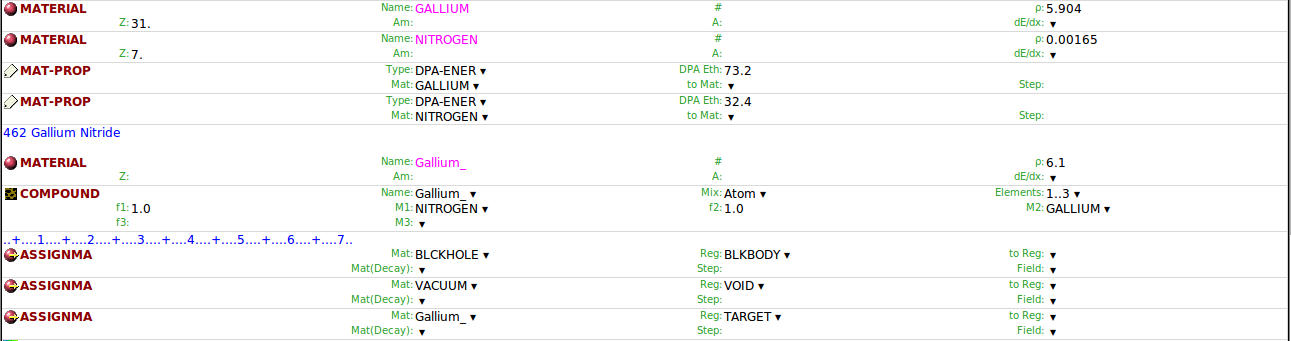
I am trying to check the DPA and NIEL for GaN
(compound semiconductor) for that I have defined the
material. Ga and N has different threshold atomic
displacement energies, i have shown in the image.
Since GaN has different structure as (100) and (111),
Is there any way to take care of that in simulation?
Thanks and Regards
Shyam
__________________________________________________________________________
You can manage unsubscription from this mailing list at https://www.fluka.org/fluka.php?id=acc_info
(image/png attachment: gan.png)